Kathmandu
Wednesday, July 1, 2026


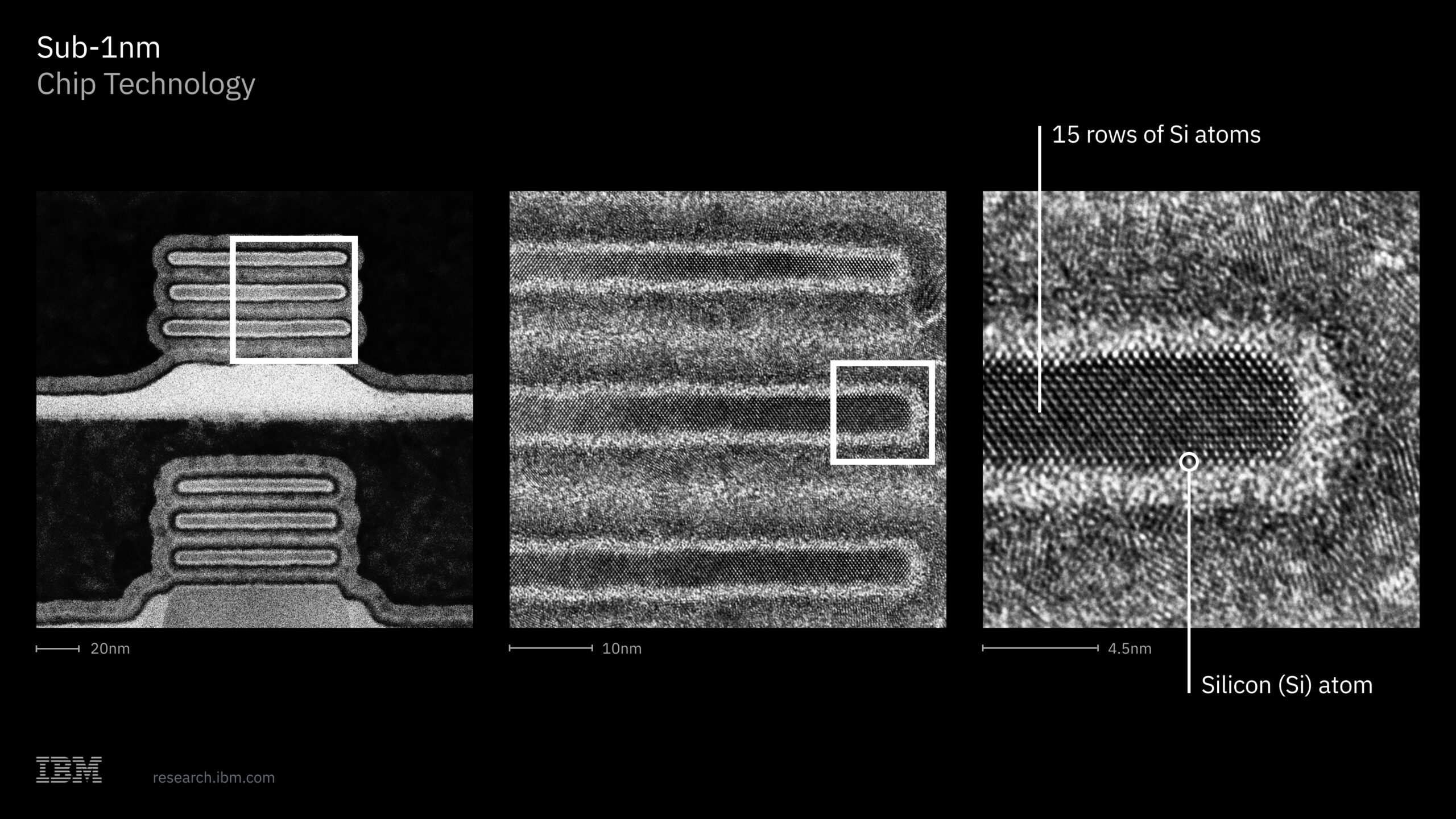
NEW YORK: IBM has unveiled what it says is the world’s first sub-1 nanometer chip technology, introducing a 0.7-nanometer (7-angstrom) architecture designed to significantly improve computing performance and energy efficiency for artificial intelligence (AI) and enterprise applications.
The new nanostack architecture uses a three-dimensional transistor design capable of fitting nearly 100 billion transistors onto a chip the size of a fingernail.
According to IBM, the technology delivers up to 50 percent higher performance or 70 percent greater energy efficiency than its 2-nanometer chips while increasing on-chip memory density by 40 percent.
The company also announced that the technology, developed at its semiconductor research facility in Albany, New York, could reach production within about five years. IBM said the breakthrough is expected to extend chip scaling for another decade as demand for AI computing continues to grow and is being developed in collaboration with semiconductor equipment partners including ASML, Lam Research, Tokyo Electron, and SCREEN Semiconductor Solutions.